
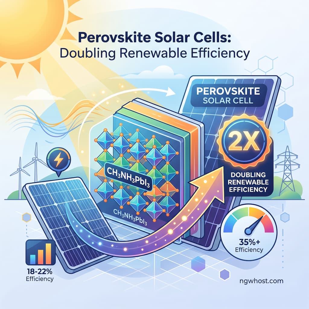
Perovskite Solar Cells: Doubling Renewable Efficiency
The global transition toward clean, sustainable energy has reached an unprecedented scale. Over the past two decades, crystalline silicon photovoltaic (PV) technology has served as the undisputed workhorse of the global solar revolution. Silicon panels have populated utility-scale desert arrays, commercial rooftops, and residential installations worldwide, driving down the levelized cost of electricity (LCOE) to historic lows and establishing solar power as the most competitive form of new electricity generation.
However, after decades of intensive materials science and manufacturing optimization, traditional crystalline silicon technology is approaching a hard physical barrier: the Shockley-Queisser theoretical efficiency limit.
For a single-junction silicon solar cell, the theoretical maximum power conversion efficiency (PCE) is physically capped at roughly 29.4%. In commercial production, top-tier silicon panels operate at practical limits between 22% and 24%. Incremental efficiency improvements in silicon manufacturing now require immense capital expenditure, extreme chemical purification processes, and high-temperature thermal processing exceeding 1,400°C.
To double renewable efficiency, lower manufacturing costs, and unlock transformative solar form factors, the photovoltaic industry is executing a generational leap in materials science: Perovskite Solar Cells (PSCs).
Perovskites refer to a class of synthetic crystalline materials that share the distinct crystallographic structure of calcium titanium oxide (ABX3). In little more than a decade, perovskite solar cells have advanced from laboratory efficiencies of under 4% to certified single-junction records exceeding 26%—a pace of efficiency growth unprecedented in the history of photovoltaics.
More critically, by layering perovskite thin films directly on top of traditional silicon cells to create Perovskite-Silicon Tandem Solar Cells, engineers have broken the single-junction ceiling, demonstrating operational efficiencies exceeding 33% to 34% in advanced testing environments.
This post analyzes the solid-state physics of perovskite materials, evaluates the mechanics of tandem solar architectures, compares legacy silicon against perovskite PV technology, and examines the digital cloud server infrastructure required to host high-consequence clean energy telemetry platforms on ngwhost.com.
1. The Physics Bottleneck: Why Silicon Solar Has Reached Its Ceiling
To understand why the global renewable energy ecosystem is turning to perovskite crystal structures, one must examine the physical limitations of single-junction silicon semiconductors.
The Single Bandgap Constraint and Thermalization Losses
Solar radiation emitted by the sun spans a broad spectrum of wavelengths—ranging from high-energy ultraviolet (UV) and visible blue light to low-energy near-infrared (NIR) photons.
A semiconductor absorbs light based on its specific bandgap energy:
- Silicon has a fixed, unalterable bandgap of approximately 1.1 electron-volts (eV).
- When a high-energy blue photon hits a silicon cell, the excess energy above the 1.1 eV bandgap is not converted into usable electricity. Instead, it is instantly lost as waste heat through a process known as thermalization.
- Conversely, low-energy infrared photons that fall below the 1.1 eV bandgap pass straight through the silicon without exciting an electron, resulting in non-absorption losses.
This single-bandgap mismatch represents the primary physical barrier defining the Shockley-Queisser limit for single-junction silicon cells.
The Capital and Energy Intensity of Silicon Refining
Silicon is not found in its pure state in nature; it exists as silica (quartz sand).
Refining raw quartz into solar-grade polysilicon requires extreme industrial heat:
- Submerged arc furnaces running at over 1,400°C to 1,900°C.
- Complex chemical purification cycles (the Siemens process) involving hazardous silane gases.
- Energy-intensive crystal pulling and diamond-wire wafer sawing that wastes substantial raw silicon dust (kerf loss).
This high thermal and manufacturing footprint limits how fast silicon production can scale without creating significant embedded carbon debts.
Perovskite materials eliminate these physical and manufacturing constraints through tunable bandgap engineering and low-temperature solution processing.
2. Solid-State Mechanics: The Magic of the Perovskite Crystal
Perovskite solar absorbers are organic-inorganic hybrid halide materials defined by the chemical formula ABX3:
- A-Site: An organic or inorganic cation (such as Methylammonium, Formamidinium, or Cesium).
- B-Site: A divalent metal cation (primarily Lead or Tin).
- X-Site: A halide anion (such as Iodine, Bromine, or Chlorine).
This unique crystal lattice provides four remarkable optoelectronic properties that make perovskites the ideal solar material:
1. Tunable Bandgap Engineering
Unlike silicon’s rigid 1.1 eV bandgap, chemical engineers can continuously tune the bandgap of perovskites between 1.2 eV and 3.0 eV simply by altering the ratio of halides (e.g., swapping Iodine for Bromine) and cations.
This allows scientists to engineer custom perovskite layers that capture specific segments of the solar spectrum with near-zero thermalization loss.
2. High Absorption Coefficient and Thin-Film Scalability
Perovskites absorb sunlight with extraordinary efficiency. A perovskite thin film just 0.5 micrometers (500 nanometers) thick absorbs as much visible sunlight as a traditional silicon wafer that is 150 to 200 micrometers thick.
This reduction in material thickness (over 300 times thinner than silicon) slashes raw material requirements and enables lightweight, flexible solar applications.
3. Long Charge-Carrier Diffusion Lengths and Defect Tolerance
In most semiconductor materials, microscopic lattice defects or atomic impurities act as “charge traps,” causing excited electrons to recombine before they can be collected as electrical current.
Perovskites exhibit high defect tolerance and exceptionally long charge-carrier diffusion lengths (often exceeding several micrometers). Electrons travel freely through the material with minimal resistive loss.
4. Low-Temperature Solution Processing
Perovskites can be synthesized from abundant liquid chemical precursor inks at temperatures below 100°C to 150°C.
Using standard roll-to-roll printing, slot-die coating, or chemical vapor deposition, perovskite layers can be printed directly onto flexible plastic substrates, architectural glass, or existing silicon wafers at a fraction of the thermal energy required for silicon.
3. The Tandem Architecture: Breaking the Efficiency Ceiling
The fastest commercial pathway for perovskites is not replacing silicon entirely, but augmenting it through Perovskite-Silicon Tandem Solar Cells.
In a tandem solar configuration, two distinct solar cells with complementary bandgaps are stacked on top of one another to extract maximum energy from the solar spectrum:
Tandem Solar Operating Sequence
- Top Layer (Wide-Bandgap Perovskite Cell): Positioned directly facing the sun, a top perovskite layer with a 1.7 to 1.8 eV bandgap absorbs high-energy blue, green, and UV photons, converting them into high-voltage electricity while remaining transparent to infrared light.
- Bottom Layer (Narrow-Bandgap Silicon Cell): The lower-energy infrared and near-infrared photons pass straight through the top perovskite layer and are absorbed by the bottom 1.1 eV silicon cell.
- Combined Performance: By dividing the solar spectrum between two tuned absorbers, tandem cells eliminate thermalization losses and achieve power conversion efficiencies of 30% to 35%+ in commercial architectures.
2-Terminal (2T) vs. 4-Terminal (4T) Tandem Configurations
- Monolithic 2-Terminal (2T) Tandem: The perovskite layer is grown directly onto the front surface of the silicon wafer, sharing electrical contacts. This produces a single, integrated panel that drops directly into standard solar module manufacturing lines, requiring only one inverter.
- Mechanically Stacked 4-Terminal (4T) Tandem: The perovskite and silicon cells are manufactured independently and stacked with separate electrical outputs. While mechanically more complex, 4T designs eliminate the need for strict current matching between the two layers.
4. Structural Optimization Ledger: Crystalline Silicon vs. Perovskite Tandem Solar
Evaluating the physical, economic, and operational parameters separating legacy silicon from next-generation perovskite-silicon tandem systems illustrates why renewable energy developers are investing heavily in tandem production lines.
Power Conversion Efficiency (PCE) Ceiling
- Crystalline Silicon Panels: Theoretical limit of 29.4%. Real-world commercial production tops out at 22% to 24%.
- Perovskite-Silicon Tandem Panels: Theoretical limit of 43%+. Real-world commercial pilot lines are already achieving 30% to 34% efficiency.
Thermal Processing & Manufacturing Footprint
- Crystalline Silicon Panels: High-temperature smelting (>1,400°C) with long energy-payback periods and complex supply chains.
- Perovskite-Silicon Tandem Panels: Low-temperature chemical printing (<150°C) for the perovskite layer, cutting total manufacturing energy by up to 50%.
Form Factor & Deployment Flexibility
- Crystalline Silicon Panels: Rigid, heavy glass-encapsulated panels. Restricted to flat roofs, open land, and reinforced structures.
- Perovskite-Silicon Tandem Panels: Highly versatile. Can be deployed on rigid tandem frames, flexible curved surfaces, vehicle bodies, or Building-Integrated Photovoltaics (BIPV).
Material Thickness & Raw Resource Consumption
- Crystalline Silicon Panels: Requires thick wafers (150 to 200 micrometers) of high-purity polysilicon.
- Perovskite-Silicon Tandem Panels: Micro-thin active layers (<1 micrometer), dramatically reducing raw material and supply chain vulnerability.
5. Real-World Applications: Transforming the Built Environment
The thin, lightweight, and semitransparent properties of perovskite solar cells open up vast new deployment surfaces that were previously impossible with heavy, rigid silicon panels:
Building-Integrated Photovoltaics (BIPV) and Solar Windows
Because perovskites can be formulated to be semi-transparent while tuning color profiles, they can be laminated directly into commercial architectural glass.
Skyscrapers can transform their entire glass curtain walls into gigawatt-scale clean power generators without blocking natural interior daylight.
Vehicle-Integrated Photovoltaics (VIPV)
Automotive manufacturers face severe weight and curvature constraints when adding solar to electric vehicles.
Flexible, lightweight perovskite thin films can be molded directly onto vehicle roofs, hoods, and body panels, generating 20 to 30 miles of additional driving range per day from ambient sunlight without adding aerodynamic drag or significant weight.
Space Applications and Aerospace High-Altitude Drones
Spacecraft, satellites, and high-altitude pseudo-satellites (HAPS) require ultra-high power-to-weight ratios.
Perovskite cells offer higher radiation tolerance and superior performance under extraterrestrial solar spectra compared to traditional silicon, delivering maximum electrical output per kilogram of orbital payload.
Indoor and Low-Light IoT Energy Harvesting
Perovskite bandgaps can be tuned specifically to absorb indoor LED and fluorescent lighting spectra.
Small indoor perovskite harvesters can power wireless IoT sensors, smart home devices, and electronic retail shelf labels indefinitely without requiring replaceable chemical batteries.
6. Systemic Operations: Cloud Infrastructure for High-Throughput Energy Telemetry
Deploying, monitoring, and optimizing massive utility-scale perovskite solar farms and smart-grid energy storage systems demands an underlying digital server infrastructure that prioritizes high availability, low latency, and zero-downtime execution. Modern clean energy platforms operate on sophisticated Industrial IoT (IIoT) control networks that process continuous, high-consequence data streams—ranging from string-level maximum power point tracking (MPPT) telemetry and inverter degradation analytics to real-time grid-dispatch APIs and automated weather forecasting models.
If an enterprise solar operations platform, grid-tie control gateway, or renewable energy trading system experiences database configuration drift, network latency, or server downtime during a peak generation window, the consequences are immediate. Inverter synchronization algorithms stall, localized grid substations face phase imbalances, and automated clean energy arbitrage transactions fail—incurring significant financial losses.
To eliminate this operational friction, progressive clean tech software engineering teams, utility operators, and digital platform developers deploy highly optimized, zero-downtime server architectures.
These infrastructure layers continuously monitor active API endpoints, encrypted SCADA telemetry database write paths, and high-throughput energy grid optimization nodes, ensuring processing response times stay locked within sub-millisecond thresholds regardless of data volume.
Maintaining an unassailable infrastructure perimeter is vital to eliminate bandwidth bottlenecks, protect proprietary solar plant predictive models, and preserve platform trust, driving peak structural execution across enterprise portals and hosting domains like ngwhost.com.
7. Commercial Engineering Hurdles: Durability and Lead Encapsulation
While the efficiency gains of perovskite solar cells are undisputed, commercializing perovskite technology at a global scale requires solving two primary materials engineering challenges:
- Long-Term Environmental Stability (Degradation): Early laboratory perovskites degraded rapidly when exposed to ambient moisture, oxygen, UV light, and sustained thermal stress. Solar manufacturers have engineered advanced molecular self-assembled monolayers (SAMs), 2D/3D hybrid perovskite barrier layers, and hermetic atomic layer deposition (ALD) glass encapsulants, allowing modern commercial perovskite modules to pass standard IEC 61215 accelerated aging and damp-heat durability tests (maintaining 80%+ performance over 20 to 25 years).
- Lead Sequestration & Non-Toxic Alternatives: Most high-efficiency perovskites contain trace quantities of lead in their chemical matrix. While the total amount of lead is minuscule (less than a fraction of the lead found in typical electronics solder), manufacturers are developing advanced cross-linked polymer traps that chemically bind lead during physical module damage, alongside parallel research into non-toxic tin-based perovskite alternatives.
Read More⚡ Venture Secondaries: Liquidity in Illiquid Markets
Conclusion: The New Frontier of Clean Power Generation
Perovskite Solar Cells are not an incremental improvement in panel design; they mark a fundamental physics transformation in how human civilization harvests the power of the sun. The legacy paradigm of relying exclusively on single-junction silicon wafers constrained by rigid thermodynamic ceilings is being permanently superseded by high-efficiency, multi-junction tandem architectures.
The future of renewable energy belongs entirely to the visionary materials scientists, solar developers, and data-driven platform networks that master the orchestration of perovskite thin-film technologies today.
By combining tunable bandgap engineering, low-temperature solution printing, perovskite-silicon tandem stacking, and zero-downtime digital cloud infrastructure perimeters, the international clean energy community is building an unassailable foundation for global decarbonization.
As industrial manufacturing lines scale up and commercial tandem modules deploy across utility grids, rooftops, and vehicle surfaces worldwide, clean power yields will surge to historic heights—permanently establishing Perovskite Solar Cells as the essential engine doubling renewable efficiency worldwide.
Hosting computationally intensive solar telemetry engines, processing real-time system data streams, validating cloud-scale automation pipelines, and managing ultra-secure global server frameworks requires world-class, zero-downtime infrastructure. Secure your enterprise digital data framework on an unassailable foundation by exploring the premium hosting configurations at ngwhost.com.